Home › Forums › Technical Notes › Creating Port Connector Symbols in DesignWorks™
- This topic has 0 replies, 1 voice, and was last updated 9 years, 9 months ago by
NeilMackenzie.
-
AuthorPosts
-
July 30, 2014 at 9:56 pm #823
NeilMackenzie
KeymasterCreating Port Connector Symbols in DesignWorks™
Purpose of This Note
This DesignNote describes the process of creating a port interface between an internal circuit and the parent device symbol in a hierarchical design. This information is needed primarily when creating a design “bottom up”, i.e. when you want to create a complete definition of an internal circuit before attaching it to the parent device symbol. When working “top down”, DesignWorks will automatically create a port interface for you the first time you open an internal circuit, eliminating the need to create and place Port Connector symbols manually.
Most of what is described here is condensed from the chapter “Hierarchical Design” in the DesignWorks manual.
This note applies to: Windows Macintosh DesignWorks Professional 3.0 + 3.0 + DesignWorks Lite N/A N/A LogicWorks 3.0 + 3.0 + Notes: N/A – not applicable to this version. “3.0 +” indicates version 3.0 and later. Since this note may apply to multiple versions and platforms, there may be some variation in exact configuration of menu commands and screen layouts from that shown in this note, but the same principles apply. Introduction
To connect signals across levels of hierarchy requires a Port Connector pseudo device matching each pin on the parent device symbol. This tech note describes how to create these Port Connector symbols and ensure that the connection between hierarchy levels is made correctly.
Port Connector Rules and Regulations
When making an association between the pins on a parent device symbol and the Port Connectors in the sub-circuit, DesignWorks follows these rules:
- Parent pins and port connectors are matched by name. I.e. The name of the Port Connector (applied using the pencil tool or the Name command) must match the pin name on the parent device symbol (i.e. as it appears in the DevEditor’s pin list).
- Each pin on a parent device must have one and only one matching port connector in its internal circuit. If you want to connect a parent pin to various points in the internal circuit, you must place exactly one Port Connector with a matching name, then connect the attached signal to others by name or using Page Connectors.
- Port connectors must have only one visible pin. The distinction of “visible” is made here because a bus port connector will have internal or “invisible” pins for each signal imported from the bus. This is explained further below.
Port Connector Pin Function
The pin function (i.e. input, output, etc.) for a pin on a parent device and a port connector is important.
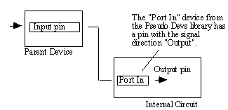
If the parent device pin is an input then the port connector in the internal circuit must have a port connector with an output pin. In this case the parent device’s input pin is driving the signal in the internal circuit. To connect a signal in an internal circuit with an input pin on a parent device use the “Port In” connector in the “Pseudo Devs” library.

If the parent device pin is an output then it must be driven by the internal circuit, the internal circuit’s port connector should have an input pin. To connect a signal in an internal circuit with an input pin on a parent device use the “Port Out” connector in the “Pseudo Devs” library.
If the parent device pin is Bidirectional then the internal circuit’s port connector should have a bidirectional pin as well.
NOTE: When the pin function on a port connector is examined from the schematic module via the Pin Info dialog, the function shown is that of the parent type pin. This means that if the parent type pin is an input then the matching internal circuit port connector’s pin will show as an input pin in the pin info dialog. If you examine the port connector in the DevEditor’s pin palette, the same pin will show as an output.
For normal signals (i.e. not buses) you can simply use one of the Port devices from Pseudo Devs library: Port Bidir, Port In or Port Out. These need to be named to match the pin names of the parent device.

Bus Port Connectors
A bus port connector must have an internal pin for each bussed signal that is exported from the internal circuit to the parent’s bus pin. Since a bus in DesignWorks may contain an arbitrary collection of signals, it is not possible to provide a bus port connector in the “Pseudo Devs” library. For Bussed signals the Port Connector must be customized for each different bus.
A Bus Pin has an internal pin for each signal that is exported from the internal circuit to the parent’s bus pin.
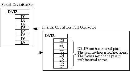
For example to export an 8 bit data bus in the internal circuit requires a bus port connector with 9 pins. One visible bus pin and 8 invisible bus internal pins.
DATA[ D0, D1, D2, D3, D4, D5, D6, D7 ]
Here the bus pin is “DATA” and the bus internal pins are “D0..D7”

As with signal port connectors, explained at the start of this tech note, the bus internal pin’s pin function on the parent device needs to correspond to the bus internal pin’s pin function on the bus port connector in the internal circuit. E.g. An input pin on the parent must correspond to an output pin on the port connector.

In this example we are building a data bus port connector which will be placed in an internal circuit. These data signals are bidirectional so we will want the pin function of all the pins in the bus port connector and the parent device’s bus internal pins to be bidirectional. All pin functions inside a bus port do not need to be the same, you may mix pin functions within a bus, some input, some output etc…. Remember that the pin function of the port connector bus internal pins must correspond to the parent device’s bus internal pins.
NOTE: The Bus Port Connector does not export all the signals in the attached bus, only the ones for which is has explicit Bus Internal pins.
Creating a Bus Port Connector in DevEditor
To create a bus port connector for the above example:
1. Select the DevEditor module from the Tools menu.
2. From the DevEdit menu select “Add Pins…”
3. Enter the string “DATA[D0..D7]”. See manual page 227 for Add Pins syntax.
4. For each bus internal pin set the pin function to Bidirectional, as follows:
a) Open the pin info palette by double clicking on the first internal pin name from the DevEditor’s pin list. In this example it is D0.
b) Use the pin function pop-up menu located in the center of the dialog to select Bidirectional for the pin function.
c) Press the Enter key (not return) to step to the next pin in the list.
5. Create a symbol for the connector, perhaps a simple rectangle.
6. Select the bus pin, DATA in the pin name list.
7. Place a bus pin from the DevEditor’s tool palette.
8. Set the primitive type for the device.
a) Select “Subcircuit & Part Type…” from the DevEdit menu.
b) From the “Subcircuit & Part Type” dialog select “Primitive, Use Caution”
c) From the pop-up choose “PORT CONNECTOR”.
d) Select “Done”.
9. From the “File” menu choose “Save Part As…”
10. Choose your working library to save the part.
11. Close the DevEditor window.
12. Place your new Bus Port Connector in your internal circuit.
NOTE: The pin name of the bus pin itself (in this case “DATA”) is not important. The association between the Bus Port Connector and the parent bus pin is made by the name applied to the Bus Port Connector symbol itself. I.e. The same Bus Port Connector symbol can be used for any bus with the same internal signal names.
-
AuthorPosts
- You must be logged in to reply to this topic.


